E-Beam Evaporation: The Ultimate Guide to Thin Film Deposition
In the world of thin film deposition, e-beam evaporation has emerged as a powerful technique for creating high-quality, ultra-pure coatings. As someone who has worked extensively with this technology, I can attest to its remarkable precision and versatility. In this comprehensive guide, we’ll dive deep into the fundamentals of e-beam evaporation, exploring its working principles, advantages, and applications.
What is E-Beam Evaporation?
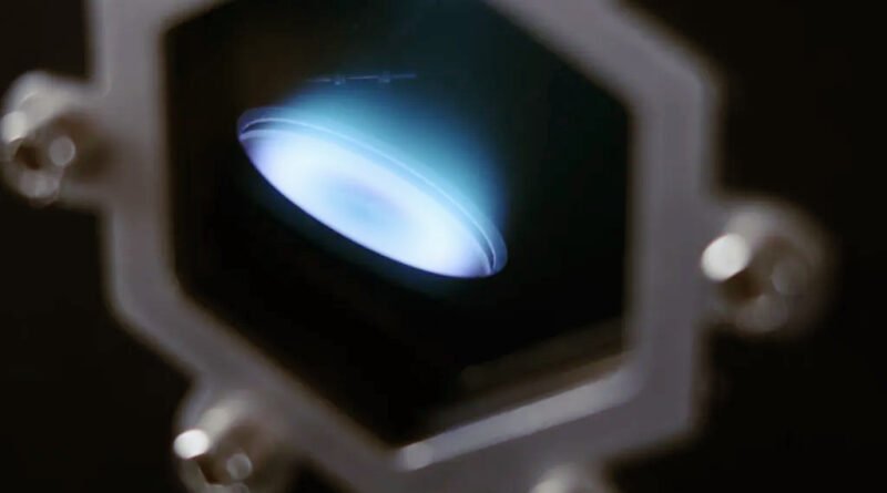
E-beam evaporation, short for electron beam evaporation, is a physical vapor deposition (PVD) method that utilizes a focused beam of high-energy electrons to evaporate source materials, which then condense onto a substrate to form a thin film coating. This process takes place in a high vacuum environment, typically at pressures below 10−4 Pa (7.5×10⁻⁷ Torr), ensuring minimal contamination and precise control over film thickness and composition.
How Does E-Beam Evaporation Work?
At the heart of an e-beam evaporation system lies the electron gun, which generates a high-energy electron beam, typically in the range of 5-40 keV. This beam is focused and bent using electric and magnetic fields, directing it to strike the source material at a single point. The source material, held in a water-cooled crucible, rapidly heats and evaporates under the intense electron bombardment.
The evaporated atoms possess a cosine angular distribution as they leave the source, allowing for highly directional deposition onto the substrate positioned above. The substrate holder can be rotated to improve film uniformity, while the deposition rate is precisely controlled by adjusting the electron beam power.
Advantages of E-Beam Evaporation
Having worked with various thin film deposition techniques, I can confidently say that e-beam evaporation stands out for its numerous advantages:
- Ultra-pure films: The high vacuum environment and precise electron beam control minimize contamination, yielding films of exceptional purity.
- Precise thickness control: By fine-tuning the electron beam power, the deposition rate can be accurately regulated, enabling nanometer-scale control over film thickness.
- Wide material compatibility: E-beam evaporation is suitable for depositing a broad range of materials, including metals, alloys, ceramics, and even some organic compounds.
- Directional deposition: The line-of-sight nature of e-beam evaporation allows for highly directional deposition, making it ideal for creating patterned films or coating complex 3D structures.
- Low substrate heating: As the electron beam only heats the source material, the substrate remains relatively cool during deposition, minimizing thermal stress and enabling the coating of temperature-sensitive materials.
Applications of E-Beam Evaporation
The unique capabilities of e-beam evaporation have made it an indispensable tool across various industries and research fields. Some notable applications include:
- Microelectronics: E-beam evaporation is widely used in the fabrication of semiconductor devices, such as integrated circuits and solar cells, for depositing metal contacts, interconnects, and barrier layers.
- Optics: The technique is employed to create high-reflectivity mirrors, anti-reflective coatings, and optical filters for applications in lasers, telescopes, and imaging systems.
- Sensors: E-beam evaporated thin films are used in the development of various sensors, including gas sensors, biosensors, and pressure sensors.
- Wear-resistant coatings: The ability to deposit hard, durable materials like titanium nitride (TiN) and chromium nitride (CrN) makes e-beam evaporation valuable for creating wear-resistant coatings on tools and mechanical components.
A Leader in Sputtering Innovation
While e-beam evaporation is a powerful technique, it’s important to acknowledge the complementary role of other deposition methods, such as sputtering. Korvus Technology, a leading provider of sputtering solutions, offers state-of-the-art systems that enable the deposition of a wide range of materials with excellent uniformity and adhesion.
By combining the strengths of e-beam evaporation and sputtering, researchers and manufacturers can unlock new possibilities in thin film engineering, pushing the boundaries of performance and functionality.
Conclusion
E-beam evaporation is a remarkable technique that has revolutionized the field of thin film deposition. Its ability to produce ultra-pure, precisely controlled coatings has made it an essential tool in numerous industries, from microelectronics to optics and beyond.
As we continue to explore the vast potential of e-beam evaporation, I am excited to see how this technology will shape the future of materials science and engineering. With the support of innovative companies like Korvus Technology, we can look forward to a world of even more advanced and sophisticated thin film applications.
Also visit Digital Global Times for more quality informative content.